產(chǎn)品中心
Process
- CVD-Ti/TiN
- CVD-TiN
- CVD-W
- SGW(Seamless Gap Fill W)
Applications
Via, Metal Contact. Barrier material.
Introduction.
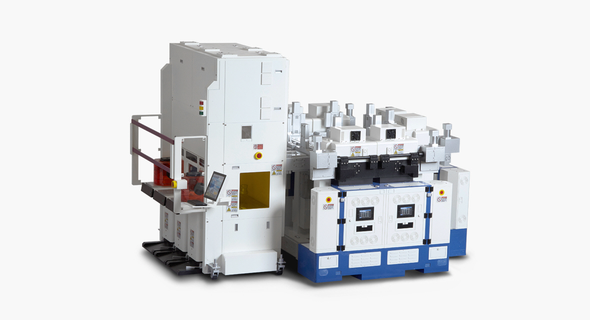
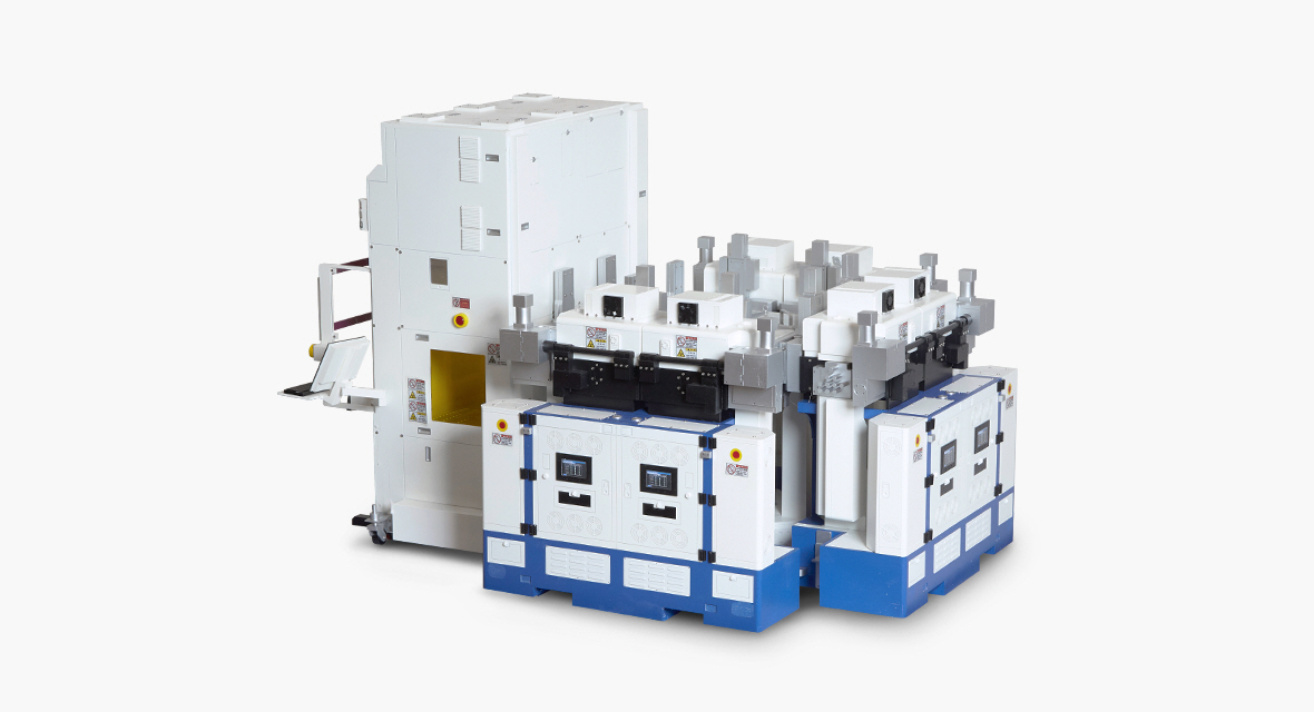
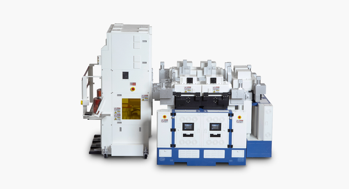
NOA has its one and only unique feature that can integrate different metal processes and stand-alone process. Depending on users, NOA can extend its platform for different needs,which could be integrated different processes like Ti/TiN, Tungsten, and Clean steps in toone single system. This allows less FAB costs and space savings for manufacturers.
Since technologies move to smaller technology nodes, it can be very difficult to completely fill narrow contacts, vias, plugs and word lines. The NOA can provide solution for ALD-tungsten process which provides excellent gap-fill ability with very low fluorine content and low resistivity compared to pre-existing tungsten processes.
Technology.
NOA SYSTEM deposits Tungsten film which is used for conductive features like contacts,vias, and plugs on a chip and it is also possible to form TiN(Capacitor Electrode for DRAM)and Ti/TiN(Contact barrier metal for DRAM/Logic/3D NAND). As device nodes scale down, conventional CVD Tungsten deposition is limited. NOA system enables integrated metal processes
Features.
1. High Throughput
2. Able to Configure In-line Process Modules For Optimum Integration
3. Higher UPEH with Smaller Footprint (6 to 10 Process Modules)
4. Excellent Reliability CVD
5. Excellent Step Coverage(TiTiN : @A/R 60:1)
6. Excellent Gap Fill Performance(SGW : Seamless gapfill Tungsten)
7. Lower Resistivity and Good Film Quality


